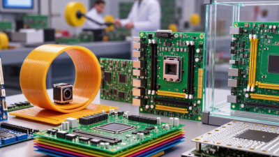
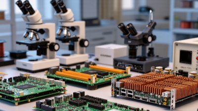
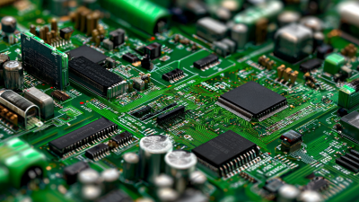
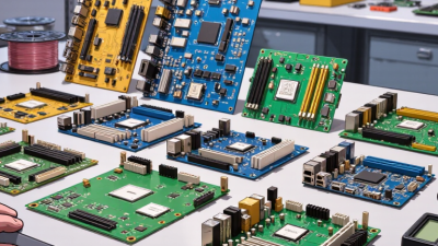
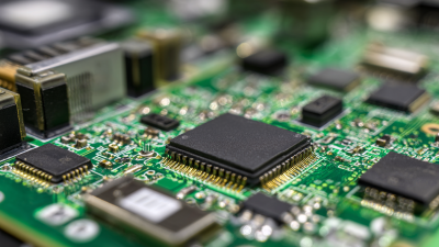
An Electronic Circuit Board is the physical platform that connects, supports, and organizes electronic components. It may appear to be a flat green panel, but its copper pathways perform precise electrical work. These pathways carry signals and power between chips, resistors, capacitors, connectors, and other parts. Without this structure, modern devices would be difficult to assemble, repair, or scale.
Look closely at a circuit board. Thin copper traces run between tiny solder joints. Small holes may connect several layers inside the board. A printed label can identify component positions, polarity, or testing points. The board’s material also provides insulation and mechanical strength. Common examples include single-sided, double-sided, and multilayer boards. Each design suits different levels of space, speed, heat, and manufacturing complexity.
The term can seem simple. It is not. Board performance depends on layout accuracy, material selection, solder quality, heat control, and inspection. Engineers often use design software and electrical testing before production begins. Even then, a minor trace defect can interrupt an entire product. A careful explanation should also admit one limitation: no board design is perfect for every application. A low-cost board may work well in a household device, yet fail under severe vibration or high temperatures. Understanding these trade-offs makes the subject more practical. It also helps readers evaluate board quality beyond color, size, or appearance.
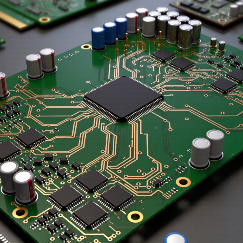
An electronic circuit board is a rigid or flexible platform that connects electronic components. It may contain chips, resistors, capacitors, connectors, and protective coatings. Thin copper traces carry electrical signals between these parts. Together, the board creates an organized path for power, data, and control signals. Without this structure, a device would need many loose wires.
The basic purpose of an electronic circuit board is to make a circuit stable, repeatable, and easier to assemble. It holds components in precise positions and links them through designed pathways. For example, a control board may receive a sensor signal, process it, and activate a motor. In practical repair work, technicians inspect solder joints, damaged traces, and overheated areas. Small faults can stop the entire device. A loose connection matters.
Circuit boards also help manage space, heat, and electrical interference. Their layout affects performance, safety, and maintenance. Good designs separate sensitive signals from noisy power sections. They may also include holes, labels, fuses, and grounding areas. However, no board is perfect. A compact layout can be efficient but difficult to repair. Heat may slowly weaken materials, even when the board looks normal. This is why testing should consider both visible damage and hidden electrical faults. The definition sounds simple, but real boards involve compromises that deserve careful review.
An electronic circuit board is a structured platform that mechanically supports electronic components and electrically connects them through conductive copper pathways. Copper thickness affects current-carrying capacity, heat dissipation, and the durability of the board.
Reference: Common nominal copper weights are approximately 0.5, 1, 2, and 3 ounces per square foot, corresponding to copper thicknesses of about 17, 35, 70, and 105 micrometres.
An electronic circuit board is a flat platform that connects and supports electrical components. It uses copper traces to carry power and signals between connection points. The board material provides insulation and mechanical strength. A protective solder mask helps prevent accidental electrical contact.
Resistors control current and divide voltage. Capacitors store small amounts of energy and reduce sudden voltage changes. Inductors resist rapid changes in current, especially in filtering circuits.
Diodes guide current in one direction, while integrated circuits perform processing, timing, or control functions. Connectors link the board to batteries, sensors, displays, or other boards.
Crystals may provide accurate timing. Fuses can interrupt current during a serious fault. Small markings matter. They help technicians identify values, polarity, and test points during inspection.
Tips: Check polarity before powering a board. Look for cracked solder joints, loose connectors, and burned areas. A multimeter can reveal unexpected resistance or missing voltage. Keep the work area dry and use proper grounding. In bench testing, a board may appear clean but still contain a hidden fault under an integrated circuit. I have found that visual inspection alone is not enough. Testing each section slowly is more reliable, although it can feel unnecessarily cautious. Some troubleshooting steps also need improvement when measurements are recorded poorly.
An electronic circuit board is a controlled path for electrical signals. Copper traces connect components, while insulating layers keep unwanted current away. A signal usually begins at a power source or driver. It then travels across a trace, through a via, or between copper planes.
The signal is not simply “moving electricity.” Its changing electric field travels through the surrounding dielectric material. Trace width, copper thickness, and distance from the reference plane affect impedance. A sharp corner can add a small discontinuity. A long parallel trace can create crosstalk. It may look harmless.
On a workbench, engineers often check continuity first. That test only proves a basic connection. It does not confirm clean signal timing. For faster circuits, an oscilloscope can reveal ringing, overshoot, and delayed edges. A poorly placed return path may force current around a gap, increasing electromagnetic noise.
The 2024 Printed Circuit Board Market report estimated the global market at about 76.9 billion dollars in 2023, with projected growth near 5.6% annually through 2030. The IPC 2024 Global Electronics Industry Survey also identified ongoing pressure to improve manufacturing quality and reliability. These figures reflect a practical reality: denser boards require tighter signal control. Designers must consider the entire route, not only the visible copper line. I sometimes find that the simplest layout is not the quietest one. Reviewing the return path can change the result.
An electronic circuit board connects components through copper pathways on an insulating base. In practice, its layout controls signal quality, heat movement, repair access, and production cost. Rigid boards suit computers, appliances, vehicles, and industrial controllers. Flexible boards bend inside cameras, medical instruments, and compact wearable devices. Rigid-flex boards combine both benefits, but they demand stricter design checks.
Single-layer boards remain useful for simple controls and low-cost products. Double-layer boards support denser routing and moderate circuit complexity. Multilayer boards place copper paths between insulating layers, saving space in advanced equipment. High-density interconnect boards use tiny vias and narrow tracks. They support smaller devices, although inspection becomes harder. MarketsandMarkets projected the global printed circuit board market to reach about 95.4 billion dollars by 2028. Its 2023 analysis identified consumer electronics, communications, automotive systems, and industrial equipment as major application areas.
Tips: Match the board type to heat, vibration, moisture, and repair needs. Check trace width before selecting components. Leave test points near critical signals. A board may pass electrical tests yet fail after repeated heating. That uncomfortable detail deserves attention. IPC design and acceptability guidance can improve consistency, but standards cannot replace real-world testing. Prototype with the final enclosure, connectors, and expected cable movement. Otherwise, a perfect schematic may produce an unreliable product.
An electronic circuit board is a layered platform that connects and controls electronic components. Its copper traces carry power and signals across a compact surface. Manufacturing begins with insulating laminate, copper foil, and carefully drilled holes. Machines form the circuit pattern through imaging, etching, and plating. Clean rooms help prevent dust from damaging fine connections. Small defects can become expensive failures.
During assembly, solder paste is placed on exposed pads before components are positioned. A controlled heating profile melts the paste and forms each joint. Inspectors examine solder shape, component direction, and missing parts. Automated optical inspection finds many errors, but it cannot understand every design risk. Manual review still matters. The process is not perfectly linear.
Testing may include continuity checks, insulation measurements, and powered functional tests. X-ray inspection can reveal hidden solder voids beneath difficult packages. Engineers record voltage readings, temperature levels, and failure locations. A board can pass inspection and still fail in the field. We sometimes overtrust automated equipment. When a failure appears, technicians should reproduce it before changing parts.
Maintenance begins with visual checks for corrosion, cracked solder, loose connectors, and darkened areas. Dust and moisture should be removed using approved tools and controlled procedures. Technicians compare new measurements with earlier service records. Thermal cycling can expose weak joints that normal operation misses. Repairs require traceable notes, calibrated instruments, and careful handling against static electricity. Some boards are repaired too quickly, without identifying the original cause.
WhatsAppOffer Electronics Manufacturing All-in-One
PCBONLINE® is a registered trademark or service mark of pcb online limited or its affiliates.
Copyright © 2001-2024 Pcb Online Limited. All rights reserved