What is Pcb Printed Circuit Board and How Does it Work?
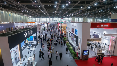
The Pcb Printed Circuit Board is an essential component in modern electronics. In 2022, the global PCB market reached approximately $68 billion, according to industry reports. This growth reflects the rising demand for electronic devices in communications, automotive, and consumer goods. Pcb Printed Circuit Boards serve as the backbone of these devices, enabling them to function efficiently.
PCBs work by connecting electronic components via conductive pathways. They support both the physical structure and the electrical connections, allowing for complex circuit designs. However, the manufacturing process can be intricate, often leading to defects. A study indicated that about 10% of PCBs have quality issues that may affect performance. Such statistics emphasize the need for stringent quality control in PCB production.
As technology advances, the Pcb Printed Circuit Board industry is facing new challenges. Innovations in materials and designs are crucial. Designers must balance functionality, cost, and reliability. While the future looks promising, industry leaders must reflect on the sustainability of production methods and materials used.
What is a PCB: Definition and Overview
A Printed Circuit Board (PCB) is a crucial component in electronics. It provides the physical foundation for electronic circuits. PCBs support and connect various electronic components using conductive pathways. These pathways are etched from copper sheets. They serve as the spine or nerve center of electronic devices.
According to a report by Research and Markets, the global PCB market is expected to reach $80 billion by 2026. This significant growth reflects the rising demand in sectors like automotive, consumer electronics, and communication. As technology advances, PCB designs become more intricate. Multilayered PCBs now allow for complex circuits to fit into smaller spaces, improving device efficiency. However, the sophistication of modern PCBs can lead to challenges in manufacturing and quality control.
Issues such as delamination and inconsistent trace width frequently arise. These challenges may lead to circuit failures or reduced performance. Manufacturers continually seek to address such problems. They invest in advanced material research and improved fabrication techniques. For instance, high-frequency PCBs demand specialized materials and precise engineering. This ongoing evolution highlights the need for expertise and innovation within the PCB industry.
The Components of a PCB: Key Elements Explained
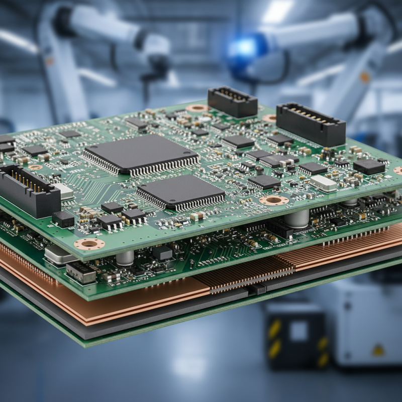
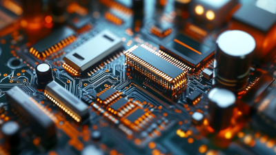
A printed circuit board (PCB) is integral to modern electronics. It serves as the backbone for various devices, connecting components like resistors, capacitors, and microchips. Each element plays a vital role in the functionality of the circuit. While PCBs can be simple or complex, understanding their components is crucial.
The primary layers of a PCB include the substrate, copper layer, and silkscreen. The substrate provides support. Common materials are fiberglass or epoxy resin. The copper layer, usually on both sides, facilitates electrical connections. This copper can also vary in thickness, impacting how signals travel. Silkscreen layers contain identifying marks, aiding in assembly. According to a recent study, the global PCB market was valued at around $60 billion in 2022, demonstrating significant growth.
Components such as capacitors and inductors affect signal behavior on the board. High-frequency applications benefit from surface-mounted devices (SMDs). Their size and placement can influence performance. Notably, a poorly designed PCB can lead to issues like electrical noise or heat dissipation challenges. These problems highlight the importance of precise engineering and the need for continuous improvement in design practices.
How PCBs are Manufactured: The Production Process
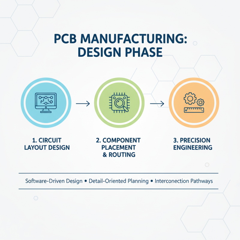
The production process of printed circuit boards (PCBs) involves several intricate steps. Initially, it begins with designing the circuit layout using specialized software. Engineers carefully plan the placement of components and the interconnecting pathways. This stage requires a keen eye for detail and precision.
Once the design is finalized, the manufacturing can commence. The process includes layering materials. Copper-clad laminates are used as substrates, which are essential for carrying electrical signals. After cutting the laminate to size, a photoresist layer is applied. This substance reacts to light, allowing for precise etching of the circuit patterns. The etching process is crucial, yet it can be variable. Sometimes, under-etching or over-etching occurs, leading to circuit flaws.
Drilling holes for component placement follows. Skilled workers must ensure that these holes are accurately positioned, as misalignment can affect functionality. After drilling, components are soldered onto the board. Automated machines often handle this step, enhancing efficiency. However, human oversight remains vital, as errors can easily arise during production. Quality checks are performed at various stages to ensure reliability. PCBs need to function flawlessly in their applications, making rigorous testing essential before they leave the factory.
Understanding PCB Functionality: How They Work in Circuits
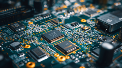
Printed circuit boards (PCBs) are essential components in modern electronics. They serve as the backbone of many devices. To understand how they work in circuits, one must consider their layered structure. Each layer consists of a substrate, conductive pathways, and insulating material. These layers work together to create a reliable framework for electronic components.
The functionality of a PCB begins with its design. Engineers carefully map out the circuit paths, ensuring that current flows efficiently. The conductive pathways, often made of copper, connect various electronic parts. Electrical signals travel along these paths, allowing the device to operate as intended. The insulating layers prevent unwanted short circuits, protecting the overall system.
While PCBs are generally reliable, they can also present challenges. Designing complex circuits may lead to overcrowded pathways. This can cause signal interference. Additionally, improper manufacturing processes can result in defects, affecting performance. Continuous testing and improvement are crucial for addressing these issues. Each iteration should aim for better efficiency and reliability in circuit functionality.
Applications of PCBs: Where They Are Used in Technology
Printed Circuit Boards (PCBs) are essential in modern electronics. They serve as the backbone for many devices we use daily. PCBs connect various electronic components through conductive pathways. This design minimizes space and enhances efficiency. In smartphones, for instance, PCBs house chips, sensors, and other vital parts. Their compactness allows for sleek device design.
In addition to smartphones, PCBs are used in numerous applications. They can be found in medical devices, automotive systems, and industrial equipment. Each sector demands reliability and precision. For example, in medical devices, a single faulty trace can affect patient outcomes. This highlights the importance of quality in PCB manufacturing.
However, the reliance on PCBs also raises questions. Are they always sustainable? Many PCBs are not biodegradable. As technology advances, the industry must focus on creating eco-friendly alternatives. The evolution of PCBs could incorporate recyclability and reduced waste. This is a critical issue for manufacturers and consumers alike.
Applications of Printed Circuit Boards (PCBs) in Technology


 Phone
Phone WhatsApp
 Email
Email

