Envisioning Tomorrow: The Evolution and Potential of PCB Board Technology
In the ever-evolving landscape of electronics, PCB board technology stands at the forefront, quietly revolutionizing the way devices are designed and integrated into our lives. As we envision tomorrow, it becomes crucial to understand not only the historical evolution of PCB boards but also their immense potential in shaping a sustainable and innovative future. From the humble beginnings of simple circuit patterns to the complex, multi-layered architectures that now support cutting-edge applications in various industries, PCB boards have undergone remarkable transformations. This guide aims to illuminate the pivotal role of PCB technology in modern electronics, exploring its advancements, challenges, and the limitless possibilities that lie ahead. Join us on this journey as we delve into the world of PCB boards and their impactful contributions to the technological advancements of tomorrow.
Common Issues Faced in Traditional PCB Board Manufacturing Processes
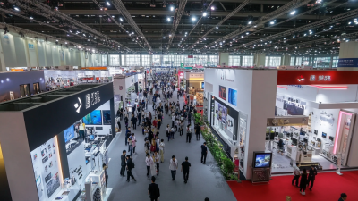
In the rapidly evolving world of electronics, traditional PCB board manufacturing processes face several significant challenges that can hinder efficiency and quality. One of the most common issues is the complexity of the design. As circuits become increasingly intricate, manufacturers often struggle to produce PCBs that meet stringent specifications without defects. The intricacies of multi-layer designs demand precise alignment, which can lead to misalignment or short circuits during the assembly process.
Another prevalent problem is the variability in raw materials. Different suppliers may provide materials with inconsistent quality, leading to performance issues in the final product. This inconsistency can result in increased rejection rates during quality control checks, wasting both time and resources. Additionally, the traditional manufacturing processes can be time-consuming, with long lead times impacting project deadlines and overall competitiveness in the market. These challenges highlight the urgent need for innovation in PCB technology to streamline manufacturing processes and improve the reliability of electronic components.
Emerging Challenges in High-Frequency PCB Applications
As the demand for high-frequency applications grows, the challenges facing PCB board technology are becoming increasingly complex. According to a report by MarketsandMarkets, the global PCB market is expected to reach $84.5 billion by 2025, with the high-frequency segment anticipated to see significant growth due to the rise of 5G technology and advanced telecommunications systems. This surge creates pressure on PCB manufacturers to design boards that minimize signal loss while maintaining thermal stability, leading to innovations in materials and manufacturing processes.

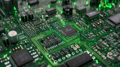
One of the emerging challenges in high-frequency PCB applications lies in the material selection. Traditional FR-4 laminates, while popular, often struggle with performance at higher frequencies, leading to issues such as increased insertion loss and poor return loss. A study published by IPC highlighted that the dielectric constant and loss tangent become critical parameters, with modern materials like PTFE and ceramic-filled composites gaining traction for their superior performance in high-frequency environments. Additionally, as circuit density increases, managing electromagnetic interference (EMI) and ensuring effective heat dissipation present further hurdles. As the industry adapts, the evolution of PCB design will continue to play a pivotal role in meeting the demands of tomorrow's technology landscape.
Environmental Concerns and Sustainable Practices in PCB Production
The production of printed circuit boards (PCBs) has long been associated with various environmental concerns, including chemical waste and resource depletion. As the demand for electronic devices continues to soar, the urgency for sustainable practices in PCB manufacturing has become increasingly apparent. Manufacturers are now exploring innovative materials that reduce environmental impact, such as biodegradable substrates and non-toxic laminates, aiming to create a greener footprint in their operations.
Moreover, recycling and reusing PCB components play a crucial role in mitigating environmental damage. By implementing closed-loop systems, companies can not only reclaim valuable materials but also significantly decrease electronic waste. This circular approach not only enhances resource efficiency but also aligns with global sustainability goals. As the industry evolves, initiatives focusing on reducing carbon emissions and promoting eco-friendly processes become vital in shaping the future of PCB technology, ultimately contributing to a more sustainable electronic landscape.
Innovations Addressing PCB Design and Durability Problems
The landscape of printed circuit board (PCB) technology is evolving rapidly, particularly in addressing design and durability challenges that have long plagued the industry. Innovations in materials science are paving the way for more robust and reliable PCBs. For instance, the integration of advanced composites and organic electronics is enhancing the durability of PCBs, making them more resilient to environmental stresses and mechanical impacts. With the PCB Cutting Tools Market projected to grow from USD 1.5 billion in 2024 to USD 2.8 billion by 2033 at a CAGR of 7.5%, the demand for precision in PCB assembly is at an all-time high.

Companies are increasingly leaning towards digital solutions to streamline their production processes. For example, recent investments in software designed to boost PCB production efficiency are transforming high-reliability sectors. Additionally, the emergence of lab-on-PCB technology is introducing innovative applications in fields such as aerospace, enabling the development of microthrusters for nanosatellites. Such advancements not only address existing durability issues but also open up avenues for new functionalities, thus illustrating the immense potential of PCB technology in the future of electronics manufacturing.
Future Trends: How Technology Is Tackling PCB Limitations
As the electronics industry continues to evolve, advancements in PCB (Printed Circuit Board) technology are pivotal in addressing its inherent limitations. A recent report by IDTechEx forecasts that the global market for PCBs will grow to over $75 billion by 2026, driven by the increasing demand for more compact, efficient, and multifunctional electronic devices. The integration of innovative materials and manufacturing processes, such as flexible and additive manufacturing techniques, is helping to push the boundaries of traditional PCB capabilities, allowing for more intricate designs and enhanced performance.
To navigate these advancements effectively, manufacturers must embrace emerging technologies. For instance, the adoption of advanced simulation and modeling techniques can significantly reduce prototype development time, allowing companies to bring products to market faster. Additionally, investing in materials that withstand higher temperatures and offer improved conductivity can further enhance PCB reliability and lifespan.
Tip: Always keep up with the latest materials science research, as breakthroughs in this area can provide competitive advantages in PCB development. Furthermore, exploring partnerships with tech startups focused on PCB innovations could uncover unique solutions to persistent challenges in circuit design and production efficiency.


 Phone
Phone WhatsApp
 Email
Email

