How to Design a Pcb Circuit Board for Beginners?
Designing a PCB circuit board can be daunting for beginners. However, with the right guidance, anyone can learn. Renowned expert Dr. Emily Zhang, a specialist in electronic engineering, once stated, “Creating a PCB circuit board is about patience and creativity.” This sentiment resonates deeply, as many beginners often underestimate the artistry involved in circuit design.
When starting, understanding the basics is crucial. A PCB circuit board is not just a flat piece of material; it’s a foundation for your project. Many newcomers frequently overlook the importance of layout and component placement. Small mistakes in this phase can lead to significant issues later. It is vital to pay attention to details. Sketching your design on paper can help establish a clearer vision.
Nevertheless, challenges will arise. Learning to use PCB design software might feel overwhelming. Accept that errors will happen; it’s part of the learning curve. Reflection on what went wrong can lead to better designs in the future. Ultimately, taking time to understand each step is essential. With practice and determination, you will master the art of designing your PCB circuit board.
Understanding PCB Basics: Types and Applications
When designing a PCB, understanding the types and applications is crucial. PCBs can be classified into several types, including single-sided, double-sided, and multi-layer boards. Each type serves specific purposes based on complexity and space constraints. A single-sided board is simpler and often used in low-power devices, while multi-layer boards offer greater connectivity.
Applications of PCBs vary widely, ranging from consumer electronics to complex industrial machinery. In consumer products, PCBs connect components and support functions. In automotive and aerospace industries, they provide reliable and durable connections. For budding designers, consider how your chosen type impacts the design process.
Mistakes are common in PCB design. You might select the wrong type for your project. Overlooking component placement can lead to errors too. Learning from these missteps is part of the journey. Embrace the challenges as a means to improve your skills and knowledge. Each iteration brings you closer to a successful design.
PCB Circuit Board Types and Their Applications
Essential Tools for PCB Design: Software and Hardware Requirements
When starting PCB design, having the right tools is crucial. Software is the backbone of your design process. Popular software tools vary widely, with prices ranging from free to costly subscriptions. According to a recent industry report, around 55% of designers prefer user-friendly software that simplifies complex tasks. Look for programs that offer simulation features. This helps in testing your designs before moving on to production.
For hardware needs, a basic setup includes a computer, design software, and a reliable 3D printer or CNC machine. These tools can assist you in creating prototypes efficiently. A study shows that approximately 70% of beginners face challenges with equipment setup. It’s vital to ensure your workspace is organized. A clutter-free area can boost focus and productivity.
Tip: Always back up your designs in multiple formats. This precaution can save you time and effort in emergencies. Learning to troubleshoot common software errors is essential. Familiarize yourself with common issues that can arise during the design process. Reflecting on your workflow can reveal areas for improvement, allowing for continuous growth in your design skills.
Step-by-Step Guide to Designing PCB Layout: From Schematic to Finished Board
Designing a PCB layout involves several essential steps. Start with a schematic diagram. This diagram outlines the connections between components. The clearer the diagram, the easier the design process will be. Use software tools available for beginners. They often have user-friendly interfaces. But, sometimes these tools can be limiting. Complex designs might require advanced features.
Once the schematic is complete, it’s time for the layout. Transfer the components from the schematic to the PCB layout. Pay attention to placement. Components should be positioned logically. Don’t forget to consider the flow of signals. It can be tempting to rush this part, but mistakes here may lead to errors later.
After placing components, route the connections. This part can be tricky. It’s important to maintain clear paths. Overlapping traces may create short circuits. Sometimes, you might find that your layout is congested. In such cases, re-evaluate your component placement. It’s a process of trial and error. Don’t be discouraged if it doesn’t come out perfect the first time. Keep refining your design until it meets your requirements.
How to Design a Pcb Circuit Board for Beginners? - Step-by-Step Guide to Designing PCB Layout: From Schematic to Finished Board
| Step |
Description |
Tools Required |
Duration |
| 1 |
Define your project requirements. |
Notepad, Project Management Tool |
1-2 hours |
| 2 |
Create a schematic diagram. |
Eagle, KiCad, Altium |
2-4 hours |
| 3 |
Choose PCB specifications (size, material). |
Internet, Datasheets |
1 hour |
| 4 |
Design the PCB layout based on the schematic. |
PCB Design Software |
4-8 hours |
| 5 |
Generate Gerber files for manufacturing. |
PCB design software |
1 hour |
| 6 |
Select a PCB manufacturer and send files. |
Internet |
1 hour |
| 7 |
Assemble components on the PCB. |
Soldering Kit, Tools |
2-5 hours |
| 8 |
Test the assembled PCB for functionality. |
Multimeter, Oscilloscope |
1-2 hours |
Key Design Considerations: Trace Width, Layer Count, and Component Placement
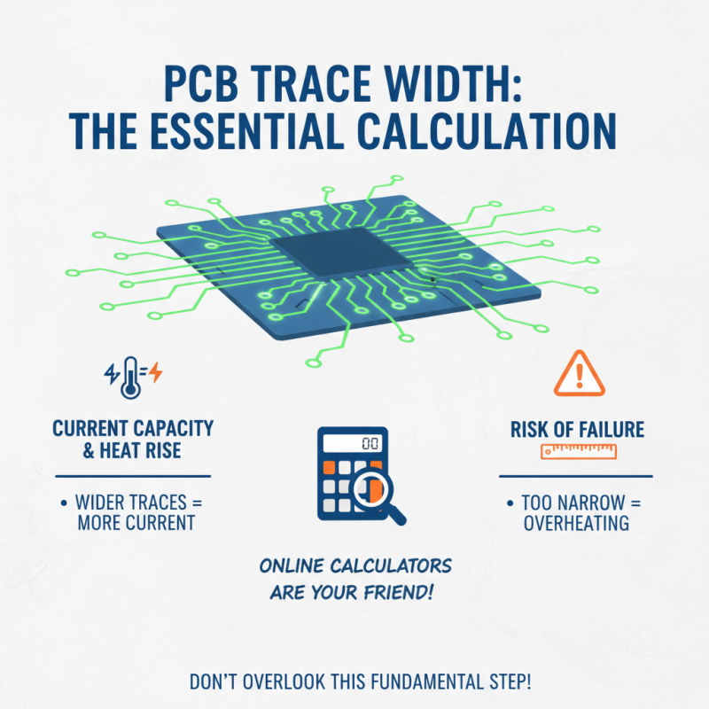
Designing a PCB circuit board can be both exciting and daunting for beginners. One critical aspect to consider is trace width. The width of traces influences how much current they can carry. If a trace is too narrow, it may overheat and fail. This is a fundamental calculation, yet many overlook it. It’s wise to refer to online calculators that help in determining the appropriate width based on current and temperature rise.
Layer count is another vital factor. A single-layer board might suffice for simple projects, but more layers can enhance design complexity. Adding layers allows for better component placement and routing options. However, more layers lead to higher costs and difficulties in manufacturing. Beginners often struggle here, learning that simplicity can sometimes lead to better functionality. Component placement affects the overall performance of the circuit too. Placing components too far apart can increase signal delay. Yet, cramming them too closely may cause unintended interference.
Reflection on errors is key in this process. Mistakes in trace width or layer count will surface during testing. Consider that a well-planned design can still fail if theoretical calculations don’t match practical outcomes. Each iteration of the design is a learning opportunity. Embrace these challenges to improve your PCB design skills.
Prototyping and Testing Your PCB: Best Practices for Beginners
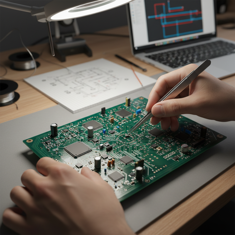
Prototyping a PCB can be exciting yet daunting for beginners. After you’ve designed your circuit, it’s time to create a prototype. Start by selecting a suitable material for your board. Common choices include fiberglass and phenolic resin. Each material has its pros and cons. Fiberglass is durable but more expensive. Phenolic is easier to work with but less robust.
Testing your prototype is crucial. Ensure all connections are secure and there are no shorts. Use a multimeter to check for continuity. This step often reveals flaws. You might find that some components don’t interact as expected. This can be frustrating but is part of the learning process. Document every test you perform. This will help identify patterns in errors.
Don’t hesitate to make adjustments to your design. It’s normal to discover improvements during testing. Redesigning might seem tedious, but it fosters a deeper understanding of circuit functionality. Remember, each mistake is a lesson. Embrace the imperfections in your work. They lead to growth and innovation in your PCB design journey.


 Phone
Phone WhatsApp
 Email
Email

